|
Mobile electronic devices, such as smartphones & tablet computers, rely heavily on the continued miniaturization of components to allow more functionality in smaller devices. Industry expects Printed Circuit Boards (PCBs) with conductive paths narrower than 10μm to mature within the next three years.
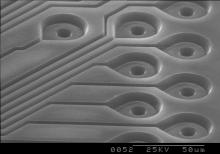
In order to support this, M-solv is working with world-leading manufacturers to develop novel High-Density Interconnect (HDI) laser material processing techniques for high-volume manufacturing of printed circuit boards. This project is specifically looking to develop a novel laser mask scanning technique for the fabrication of HDIs. The aim is to develop an ablative process, avoiding many of the environmental issues associated with the wet chemistry involved in the lithographic processes currently used. The platform is required to be able to both drill micro-vias and pattern the interconnecting traces and landing pads. |
Contact Details:
For more information please contact Dr Jon Shephard, J.D.Shephard@hw.ac.uk.

 © EPSRC Centre for Innovative Manufacturing in Laser-Based Production Processes